Reversing the RCRF-03 clicker
Jan 25, 2015Nowadays, classroom performance systems seem to be all the rage. Likewise at my uni, where I came across the Turning Technologies RCRF-03 clicker. Having read Travis Goodspeed’s hack of the RCRF-01, I decided to have a go at the newer model. The goal of this hack is to extract and reverse-engineer the executed code, and subsequently sniff or forge votes (spoiler: I failed).
Hardware
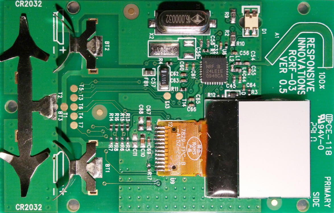
Opening up the clicker, the main chip appears to be a Nordic Semiconductor NRF
24LE1E. Some details about that chip:
- nRF24LE1 SoC
- 32-pin 5x5 QFN package
- Single package MCU, RF unit & flash memory
That last characteristic is already a big difference with the RCRF-01 model, where the flash memory was stored off-package on an SPI-addressable EEPROM.
Wiring
The datasheet1 of our SoC reveals an SPI programming interface. If we pull
the PROG pin high and pulse RESET, certain pins get reconfigured as an SPI
slave2.
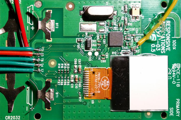
Conveniently, most of these pins are exposed through large contacts accessible via the battery compartment. Mapping them using a continuity tester, we can find out how they are connected, and connect it to some SPI-compatible tool such as the Bus Pirate:
| Functionality | MCU pin | Test point | Bus Pirate lead |
|---|---|---|---|
| FCSN | P1.1 | T7 | CS (white) |
| FMISO | P1.0 | T4 | MISO (black) |
| FMOSI | P0.7 | T6 | MOSI (grey) |
| FSCK | P0.5 | T5 | CLK (purple) |
| VCC | T1 | 3.3V (red) | |
| GND | T2 | GND (brown) | |
| PROG | T3 | 3.3V (red) | |
| RESET | AUX (blue) |
Only the RESET pin is not exposed (it is hard-wired to VCC using a 4.7kΩ
resistor), but as it turned out you don’t really have to pulse this pin as
detailed in the datasheet; rebooting the device while PROG is active suffices.
Connecting the PROG pin directly to the power supply permanently pulls it
high; this is fine for programming purposes.
As the SoC works between 1.9V and 3.6V (by default the clicker is equipped with 3V CR2032 batteries), and has a low power consumption, I wired it directly to the Bus Pirate’s integrated power supply (remember to enable that peripheral).
Lastly, I also connected the blue AUX connector to the RESET pin of the MCU
so I could accurately pulse it, but as explained before that wasn’t really
necessary.
Software
SPI is a simple interface, but allows for different modes selecting clock polarity and phase. By default, the nRF24LE1’s SPI slave starts in mode 03. I used the following settings for the Bus Pirate:
- speed: 125 KHz
- clock polarity: idle low
- output clock edge: active to idle
- input sample phase: middle
- chip select: active low
- output type: normal (high bit = 3.3V)
As an exercise to get to know the Bus Pirate better, I decided to use the
binary interface and script
everything up. However, as soon as I got some code running, I discovered that
the RDISMB (Read DISable Main Block) bit in the Flash Status Register is set.
As the name suggests, this prevents reading from main memory through an external
interface such as SPI:
Disable flash main block access from external interfaces:
0xFF: Flash main block accessible from external interfaces
Other value: No read/erase/write of flash main block from external interfaces. Only read of info page
Can only be changed once by SPI command
RDISMB. Can only be reset by SPI commandERASE ALL
And the relevant entry at address 0x23 in the Info Page:
0x00000000 (00000)   005a4330 54383231 02173e4f 775f6092
0x00000010 (00016)   26b14f0d 0affffff ff82ffff ffff0000
0x00000020 (00032)   ffffff00 ffffffff ffffffff ffffffff
I haven’t found a way around this protective bit. It is obviously impossible to
change its setting in the FSR, just as writing the underlying Info Page entry
doesn’t do anything. The only apparent way to clear this bit is to issue the
ERASE ALL command, but that kinda defeats the purpose…
As a last resort, I tried passively sniffing the SPI bus when executing the code, but the internal SPI bus doesn’t seem to be exposed when operating normally.
Wrapping up
In conclusion, it seems like Nordic has upped their game and protected their
code better. Circumventing the RDISMB restriction doesn’t seem very easy. For
example, Bunnie’s UV hack
wouldn’t apply because the info page is stored in the main flash. Racing to
access memory before the FSR is initialized can’t work because RDISMB is
enabled by default.
A possible path forward would be to gain access to the firmware upgrade code
path, if that even exists (I assume so because of the exposed SPI connectors).
Or trigger unintended behaviour by altering values in the writeable part of the
Info Page. A more far fetched alternative is to try to glitch the processor when
issuing an ERASE ALL command. But that’s taking it to a whole new level…
I’ve put the code I’ve developed on Github. It’s a comprehensive example of how to use the Bus Pirate’s binary SPI mode, and how to contact the nRF24LE1. Although it’s a non-modular piece of code, it is pretty well documented and easy to read (even though it’s written in Perl – don’t let that scare you!).
I consulted version 1.6 of the datasheet.
[return]- See page 77, section 6.3.5.1. [return]
- See page 150, section 18.3.2. [return]